Stackup
# Copyright 2026 Helge Gehring, Simon Bilodeau and contributors.
# Licensed under the Apache License, Version 2.0.
# ---
# jupyter:
#   jupytext:
#     text_representation:
#       extension: .py
#       format_name: percent
#       format_version: '1.3'
#   kernelspec:
#     display_name: Python 3
#     language: python
#     name: python3
# ---Stackup
A Stackup describes how the 2D layers in your layout extend into 3D — what
material lives at what height, how its xy footprint morphs with z, and which
entries override which. From the same Stackup you can currently produce either of two
outputs:
3D:
stack.resolve(cell)returns aResolvedStackupdescribing how each layer polygon should be extruded and cut against the others using a CAD tool.2D:
stack.resolve_cutline(cell, cutline)orstack.resolve_cross_section(cs)returns aResolvedStackup2Dcontaining the (already processed) 2D polygons of the cross-sectional view.
Both outputs share the same minimalistic painter’s-algorithm metadata: mesh_order,
keep, and cut_by. This page works through both outputs on a small but
realistic silicon-photonic stack: a rib waveguide with a TiN heater wired
out to a metal pad.
from enum import Enum

import matplotlib.pyplot as plt

import gdswell as gw
A silicon-photonic PDK
A handful of layers is enough to express a complete rib-waveguide device.
For the bulk media (Si substrate, buried oxide, oxide cladding) we use the
smart AllLayers().bbox() recipe as the xy footprint: it expands at resolve
time to the bounding box of every shape in the cell, so the bulk bodies
automatically grow to enclose whatever the device draws — no dedicated
“device extent” layer required.
class PDK(gw.Layer, Enum):
    WG = (1, 0)  # full-Si rib (220 nm)
    SLAB = (2, 0)  # partial-etch Si slab (70 nm) under and beside the rib
    HEATER = (10, 0)  # TiN heater above the rib
    VIA1 = (11, 0)  # via from heater pad to METAL1
    METAL1 = (12, 0)  # routing metal
Building entries
A StackupEntry is one logical 3D body. Currently this is a name plus a z_to_layer dict
mapping absolute z values (µm) to LayerBase recipes (with room to expand to more intricate
geometries).
The convenience constructor
StackupEntry.uniform(name, layer, zmin, zmax)builds a 2-key entry with vertical sidewallsPassing the dict directly lets you vary the xy recipe with z to produce slanted sidewalls or a topology that morphs between the keys.
# Bulk media — substrate, buried oxide, oxide claddings. All use the
# `AllLayers().bbox()` smart recipe, which resolves to the bounding box of
# every shape in the cell — so the cross-section will show them filling the
# whole frame regardless of what the device draws.
device_extent = gw.AllLayers().bbox()
substrate = gw.StackupEntry.uniform("Substrate", device_extent, -2.0, -1.0)
box = gw.StackupEntry.uniform("BOX", device_extent, -1.0, 0.0)
lower_clad = gw.StackupEntry.uniform("Lower_clad", device_extent, 0.0, 1.5)
upper_clad = gw.StackupEntry.uniform("Upper_clad", device_extent, 1.6, 2.5)

# Silicon: a 70 nm slab and the 220 nm rib that sits on top of it. The rib
# uses a 50 nm-per-side slanted sidewall via a z-varying recipe.
si_slab = gw.StackupEntry.uniform("Si_slab", PDK.SLAB, 0.0, 0.07)
si_rib = gw.StackupEntry("Si_rib", {0.0: PDK.WG, 0.22: PDK.WG.size(-0.05)})

# TiN heater, a via column, and a metal-1 pad.
heater = gw.StackupEntry.uniform("Heater", PDK.HEATER, 1.5, 1.6)
via1 = gw.StackupEntry("Via1", {1.55: PDK.VIA1, 2.5: PDK.VIA1.size(0.2)})
metal1 = gw.StackupEntry.uniform("Metal1", PDK.METAL1, 2.5, 3.5)
Composing StackupEntries into a Stackup with + and -
Stackup composition is strict painter’s order (left-to-right). + appends
an entry with keep=True. - appends it with keep=False: this is used as
a optional shortcut to
indicate that an entity should participate in later cut_by computations, while not being
emitted as an output volume. Use parentheses for explicit grouping when mixing the two.
stack = substrate + box + lower_clad + upper_clad + si_slab + si_rib + heater + via1 + metal1Pretty-printing
print(stack) renders the stackup as a table in painter’s order. Uniform
entries collapse to a single zmin → zmax row; z-varying entries get one
row per z-key so slanted sidewalls and topology morphs stay visible (look
at Si_rib).
print(stack)Stackup: 9 entries (painter's order)
──────────────────────────────────────────────────────────────────────────────────────────────
# keep name z (µm) layer
──────────────────────────────────────────────────────────────────────────────────────────────
0 + Substrate -2.000 → -1.000 LayerBBox(layer=AllLayers())
1 + BOX -1.000 → 0.000 LayerBBox(layer=AllLayers())
2 + Lower_clad 0.000 → 1.500 LayerBBox(layer=AllLayers())
3 + Upper_clad 1.600 → 2.500 LayerBBox(layer=AllLayers())
4 + Si_slab 0.000 → 0.070 PDK.SLAB
5 + Si_rib 0.000 PDK.WG
0.220 LayerSize(layer=PDK.WG, dx=-0.05, dy=None, join_mode=2)
6 + Heater 1.500 → 1.600 PDK.HEATER
7 + Via1 1.550 PDK.VIA1
2.500 LayerSize(layer=PDK.VIA1, dx=0.2, dy=None, join_mode=2)
8 + Metal1 2.500 → 3.500 PDK.METAL1
──────────────────────────────────────────────────────────────────────────────────────────────
Inserting entries into an existing stackup
It is sometimes useful to add entries to an existing stack instead of completely re-creating it.
insert_before(anchor, new) and insert_after(anchor, new) return a new
Stackup with new spliced next to the slot matching anchor, targeted by either entry
name or a StackupEntry object (matched by equality).
Passing a whole Stackup splices all of its items in at once. Setting keep=False
turns everything inserted into a cutter (as if concatenated with “-”). For instance:
etch_stop = gw.StackupEntry.uniform("Etch_stop", device_extent, 1.5, 1.55)
print(stack.insert_after("Lower_clad", etch_stop))
Stackup: 10 entries (painter's order)
──────────────────────────────────────────────────────────────────────────────────────────────
# keep name z (µm) layer
──────────────────────────────────────────────────────────────────────────────────────────────
0 + Substrate -2.000 → -1.000 LayerBBox(layer=AllLayers())
1 + BOX -1.000 → 0.000 LayerBBox(layer=AllLayers())
2 + Lower_clad 0.000 → 1.500 LayerBBox(layer=AllLayers())
3 + Etch_stop 1.500 → 1.550 LayerBBox(layer=AllLayers())
4 + Upper_clad 1.600 → 2.500 LayerBBox(layer=AllLayers())
5 + Si_slab 0.000 → 0.070 PDK.SLAB
6 + Si_rib 0.000 PDK.WG
0.220 LayerSize(layer=PDK.WG, dx=-0.05, dy=None, join_mode=2)
7 + Heater 1.500 → 1.600 PDK.HEATER
8 + Via1 1.550 PDK.VIA1
2.500 LayerSize(layer=PDK.VIA1, dx=0.2, dy=None, join_mode=2)
9 + Metal1 2.500 → 3.500 PDK.METAL1
──────────────────────────────────────────────────────────────────────────────────────────────
An anchor must match exactly one target slot: an unknown anchor raises
ValueError, and so does an ambiguous one (duplicate names are legal in a
stackup, so silently picking a slot could corrupt painter’s order). Passing
the exact StackupEntry instead of a name is the way to disambiguate:
doubled = stack + si_rib  # a second "Si_rib" slot
try:
    doubled.insert_after("Si_rib", etch_stop)
except ValueError as e:
    print(e)
anchor 'Si_rib' is ambiguous: 2 slots match (indices [5, 9]); pass the exact StackupEntry or rebuild via items slicing
Stack perturbations
Both StackupEntry and Stackup are immutable: every perturbation returns a
new object and leaves the original untouched. Perturbations come in two
flavours — one acts on each entry’s xy layer recipes, the other on its
z-keys — and both compose cleanly through + / -, so you can perturb a
sub-stackup and drop it straight into a larger composition.
Transforming layers (xy)
The map_layers(fn) family rewrites the recipe side of every z_to_layer
entry while leaving the z-keys fixed. size, transformed, round_corners,
bbox, and the boolean selectors (interacting, inside, outside,
overlapping) are exactly the Smart Layer API
operations from notebook 12, lifted onto a stackup: each one applies the
corresponding LayerBase recipe transform to every entry. Calling one on a
Stackup applies it to every entry in the stack.
Here we grow both silicon layers by 100 nm per side — the recipes become
LayerSize(...) wrappers while the z-keys stay put:
silicon = si_slab + si_rib
print(silicon.size(0.1))
Stackup: 2 entries (painter's order)
─────────────────────────────────────────────────────────────────────────────────────────────────────────────────────────────────────────
# keep name z (µm) layer
─────────────────────────────────────────────────────────────────────────────────────────────────────────────────────────────────────────
0 + Si_slab 0.000 → 0.070 LayerSize(layer=PDK.SLAB, dx=0.1, dy=None, join_mode=2)
1 + Si_rib 0.000 LayerSize(layer=PDK.WG, dx=0.1, dy=None, join_mode=2)
0.220 LayerSize(layer=LayerSize(layer=PDK.WG, dx=-0.05, dy=None, join_mode=2), dx=0.1, dy=None, join_mode=2)
─────────────────────────────────────────────────────────────────────────────────────────────────────────────────────────────────────────
Transforming z-keys
shift_z(dz) translates every z-key; scale_z(factor, origin=0.0) scales
them about a single shared absolute origin
(new_z = origin + (z - origin) * factor). A negative factor mirrors the
stack in z. On a Stackup both apply uniformly to
all entries, so a sub-stackup moves or stretches as one rigid body.
The motivating use is floating one sub-stackup in z relative to another. Here
the silicon device is lifted 200 nm above the lower cladding — the Si_slab /
Si_rib z-rows shift up while the bulk media stay put:
base = substrate + box + lower_clad
device = si_slab + si_rib
print(base + device.shift_z(0.2))
Stackup: 5 entries (painter's order)
──────────────────────────────────────────────────────────────────────────────────────────────
# keep name z (µm) layer
──────────────────────────────────────────────────────────────────────────────────────────────
0 + Substrate -2.000 → -1.000 LayerBBox(layer=AllLayers())
1 + BOX -1.000 → 0.000 LayerBBox(layer=AllLayers())
2 + Lower_clad 0.000 → 1.500 LayerBBox(layer=AllLayers())
3 + Si_slab 0.200 → 0.270 PDK.SLAB
4 + Si_rib 0.200 PDK.WG
0.420 LayerSize(layer=PDK.WG, dx=-0.05, dy=None, join_mode=2)
──────────────────────────────────────────────────────────────────────────────────────────────
scale_z stretches thickness about the origin. Doubling the device about
z = 0 sends the slab top from 70 nm to 140 nm and the rib top from 220 nm
to 440 nm:
print(device.scale_z(2.0))Stackup: 2 entries (painter's order)
──────────────────────────────────────────────────────────────────────────────────────────
# keep name z (µm) layer
──────────────────────────────────────────────────────────────────────────────────────────
0 + Si_slab 0.000 → 0.140 PDK.SLAB
1 + Si_rib 0.000 PDK.WG
0.440 LayerSize(layer=PDK.WG, dx=-0.05, dy=None, join_mode=2)
──────────────────────────────────────────────────────────────────────────────────────────
Drawing the device
Th stackup itself is only a recipe. To resolve it, we need a cell. Here, we make a device with a 20 µm-long rib waveguide with a TiN heater strip running along it; both ends of the heater fan out to a metal-1 pad south of the waveguide, contacted by a small via column.
L = 20.0  # propagation length, µm
W = 8.0  # transverse half-extent, µm


@gw.cell
def device_cell(L=L, W=W) -> gw.Cell:
    """Test device.

    Arguments:
        L (float): propagation length, µm
        W (float): transverse half-extent, µm
    """
    cell = gw.Cell()

    # Si rib (500 nm) and surrounding slab (6 µm).
    cell.add_polygon([(0.0, -0.25), (L, -0.25), (L, 0.25), (0.0, 0.25)], PDK.WG)
    cell.add_polygon([(0.0, -3.0), (L, -3.0), (L, 3.0), (0.0, 3.0)], PDK.SLAB)

    # TiN heater: a 2 µm strip over the rib plus a 6 × 3 µm contact pad south of it.
    cell.add_polygon([(0.0, -1.0), (L, -1.0), (L, 1.0), (0.0, 1.0)], PDK.HEATER)
    cell.add_polygon(
        [(L / 2 - 3, -5.5), (L / 2 + 3, -5.5), (L / 2 + 3, -2.5), (L / 2 - 3, -2.5)],
        PDK.HEATER,
    )

    # Via1 (2 × 0.5 µm column) and a METAL1 pad sized like the heater pad.
    cell.add_polygon(
        [(L / 2 - 1, -5.0), (L / 2 + 1, -5.0), (L / 2 + 1, -4.5), (L / 2 - 1, -4.5)],
        PDK.VIA1,
    )
    cell.add_polygon(
        [(L / 2 - 3, -5.5), (L / 2 + 3, -5.5), (L / 2 + 3, -2.5), (L / 2 - 3, -2.5)],
        PDK.METAL1,
    )

    return cell


cell = device_cell(L=L, W=W)
Resolving in 3D
Stackup.resolve(cell) materialises each entry’s xy regions at its own
z-keys (no resampling) and emits one ResolvedPrism per slot. The
downstream 3D backend is expected to consume the output and apply cuts in
real 3D space, so .resolve itself does no 2D booleans — disjoint slots
simply omit each other from cut_by.
resolved = stack.resolve(cell)
print(f"{'name':<12s}  {'order':>5s}  {'keep':>4s}  cut_by")
print("─" * 50)
for p in resolved.prisms:
    print(f"{p.name:<12s}  {p.mesh_order:>5d}  {str(p.keep):>4s}  {p.cut_by}")
name order keep cut_by
──────────────────────────────────────────────────
Substrate 0 True (1,)
BOX 1 True (2, 4, 5)
Lower_clad 2 True (4, 5, 6)
Upper_clad 3 True (6, 7, 8)
Si_slab 4 True (5,)
Si_rib 5 True ()
Heater 6 True (7,)
Via1 7 True (8,)
Metal1 8 True ()
cut_by is a forward-only list of slot indices whose 3D bbox overlaps this
prism’s; a 3D backend subtracts those entries’ raw solids to obtain each
kept prism’s final volume.
Rendering the 3D stack with PyVista
gw.plot_stackup_3d(resolved) builds one pv.PolyData per kept prism
and returns a configured pv.Plotter. The viewer renders raw prism
bodies — it does not apply cut_by subtractions, because robust 3D
booleans on coplanar slab faces require exact-arithmetic CSG that VTK
does not provide. Painter’s-algorithm cuts are the downstream backend’s
job (e.g. meshwell); use this viewer for sanity-checking painter’s order,
layer footprints, and z-extents. The default opacity=0.3 keeps bulk
media (substrate, BOX, claddings) see-through so the rib, slab, heater,
via, and metal-1 pad stay visible through them. opacity_map is the
escape hatch for making specific prisms opaque.
import pyvista as pv  # noqa: E402

pv.set_jupyter_backend("static")  # PNG output for the static doc build

plotter = gw.plot_stackup_3d(
    resolved,
    opacity_map={
        "Si_rib": 1.0,
        "Si_slab": 1.0,
        "Heater": 1.0,
        "Via1": 1.0,
        "Metal1": 1.0,
    },
)
plotter.show()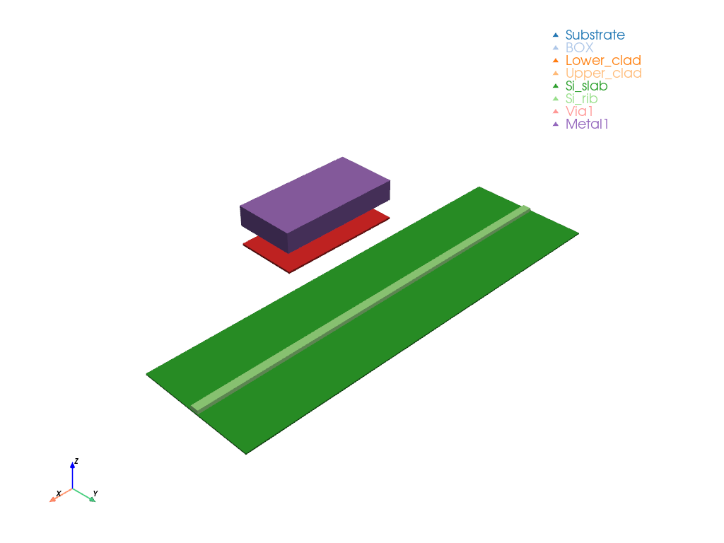
For interactive exploration during dev work, switch to
pv.set_jupyter_backend("trame") (and install trame-pyvista); the
viewer code is unchanged.
Cutting in 2D — resolve_cutline
To get a 2D cross-section, pass a cutline (two xy points in microns)
through the cell. The output ResolvedStackup2D carries per-entry
kdb.Regions in the (s, z) → (x, y) convention: the region’s x-axis
is arclength s along the cutline; its y-axis is the stackup height z.
cutline = ((L / 2, -W + 1.0), (L / 2, W - 1.0))  # transverse cut at midspan
resolved_2d = stack.resolve_cutline(cell, cutline)

# Two views: the full stack on the left, a zoom on the silicon layers on the
# right. The 220 nm rib and 70 nm slab are honest to scale, which is why they
# vanish in the full-stack view next to micron-thick claddings.
fig, (ax_full, ax_zoom) = plt.subplots(1, 2, figsize=(12, 4.5))
gw.plot_cross_section(resolved_2d, ax=ax_full)
ax_full.set_title("Full stack — transverse cut")

gw.plot_cross_section(resolved_2d, ax=ax_zoom)
ax_zoom.set_xlim(5.5, 8.5)
ax_zoom.set_ylim(-0.1, 0.35)
ax_zoom.set_aspect("auto")  # break aspect lock so the slanted rib reads clearly
ax_zoom.set_title("Zoom on the Si rib + slab")
plt.tight_layout()
plt.show()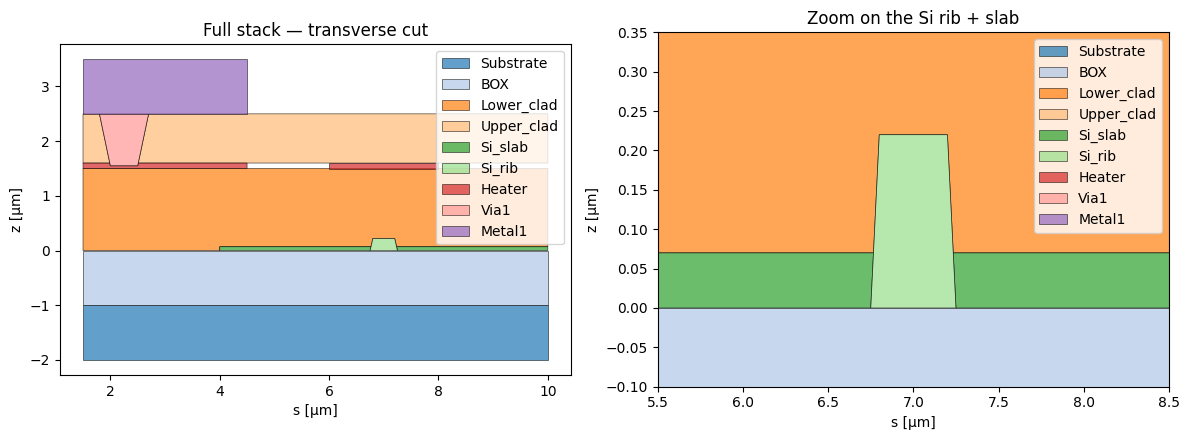
The bulk media (substrate, BOX, oxide claddings) fill the frame; on top of them you can see the heater strip, the heater contact pad with a via climbing up through the upper cladding, and the metal-1 pad capping the via. The zoom on the right reveals the 220 nm slanted-sidewall rib sitting on the 70 nm slab — both vanish in the full-stack view because they are honestly to scale next to micron-thick claddings.
Painter’s algorithm and cut_by
Later entries cut earlier ones where their 3D (or 2D) bboxes overlap.
plot_cross_section applies these cuts by default (apply_cuts=True) so
you see each prism’s final, carved patch. Compare with apply_cuts=False,
which renders the raw per-entry regions before any subtraction. This is useful
to debug painter’s order.
fig, ax = plt.subplots(figsize=(8, 4.5))
gw.plot_cross_section(resolved_2d, ax=ax, apply_cuts=False)
ax.set_title("Same stackup, apply_cuts=False (raw per-entry regions overlap)")
plt.tight_layout()
plt.show()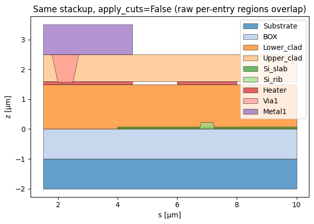
Cutting in 2D — resolve_cross_section
In many layouts, you usually already work with a CrossSection. The
convenience Stackup.resolve_cross_section(xs, s=0.0) evaluates the
CrossSection at s, builds a synthetic straight whose xy layout matches
the evaluated profile, and slices it with a perpendicular midspan cutline.
No manual cutline needed.
xs = gw.CrossSection(
    layer_sections=(
        gw.LayerSection(name="slab", layer=PDK.SLAB, width=6.0, offset=0.0),
        gw.LayerSection(name="rib", layer=PDK.WG, width=0.5, offset=0.0),
    )
)

# A trimmed stack — just the rib-waveguide layers around the silicon.
rib_stack = substrate + box + lower_clad + si_slab + si_rib
resolved_xs = rib_stack.resolve_cross_section(xs)

fig, ax = plt.subplots(figsize=(8, 3.5))
gw.plot_cross_section(resolved_xs, ax=ax)
ax.set_ylim(-0.1, 0.35)
ax.set_aspect("auto")
ax.set_title("Cross-section evaluated directly from a CrossSection (zoom on Si)")
plt.tight_layout()
plt.show()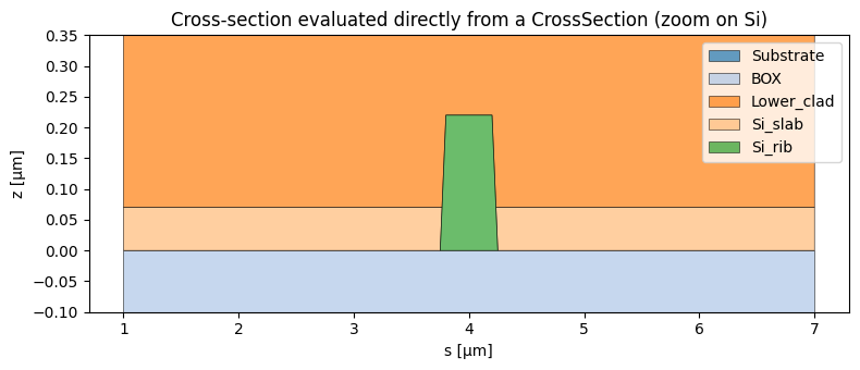
Improvements
This framework is extremely modular. We can add subclasses or keywords to StackupEntries to log information about more intricate geometries (e.g. filleted corners). We could also generate sets of StackupEntries from Stackup, for instance to emulate conformal claddings that calculate their effective footprints and levels from sets of StackupEntries in a Stackup. Alternatively, we could output “process” recipes for process simulation instead of already-rendered prisms.