PN junction depletion modulator#
/home/runner/miniconda3/lib/python3.13/site-packages/femwell/pn_analytical.py:8: SyntaxWarning: invalid escape sequence '\m'
  (3) M. Nedeljkovic, R. Soref and G. Z. Mashanovich, "Free-Carrier Electrorefraction and Electroabsorption Modulation Predictions for Silicon Over the 1–14- $\mu\hbox{m}$ Infrared Wavelength Range," in IEEE Photonics Journal, vol. 3, no. 6, pp. 1171-1180, Dec. 2011, doi: 10.1109/JPHOT.2011.2171930.
We can study the propagation constant in waveguides as a function of arbitrary physics. Here, we consider the depletion approximation to pn junctions to study how doping level and junction placement affect modulation in a doped silicon waveguide. This is a simple, yet common, approximation [1].
clad_thickness = 2
slab_width = 3
wg_width = 0.5
wg_thickness = 0.22
slab_thickness = 0.09
core = shapely.geometry.box(-wg_width / 2, -wg_thickness / 2, wg_width / 2, wg_thickness / 2)
slab = shapely.geometry.box(
-slab_width / 2, -wg_thickness / 2, slab_width / 2, -wg_thickness / 2 + slab_thickness
)
clad = shapely.geometry.box(
-slab_width / 2, -clad_thickness / 2, slab_width / 2, clad_thickness / 2
)
polygons = OrderedDict(
core=core,
slab=slab,
clad=clad,
)
resolutions = dict(
core={"resolution": 0.02, "distance": 0.5}, slab={"resolution": 0.04, "distance": 0.5}
)
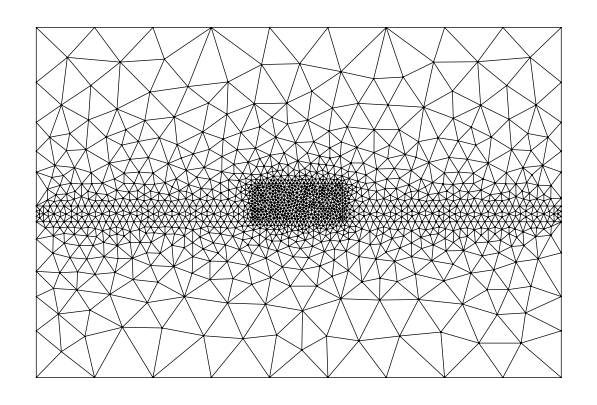
mesh = from_meshio(mesh_from_OrderedDict(polygons, resolutions, default_resolution_max=10))
mesh.draw().show()
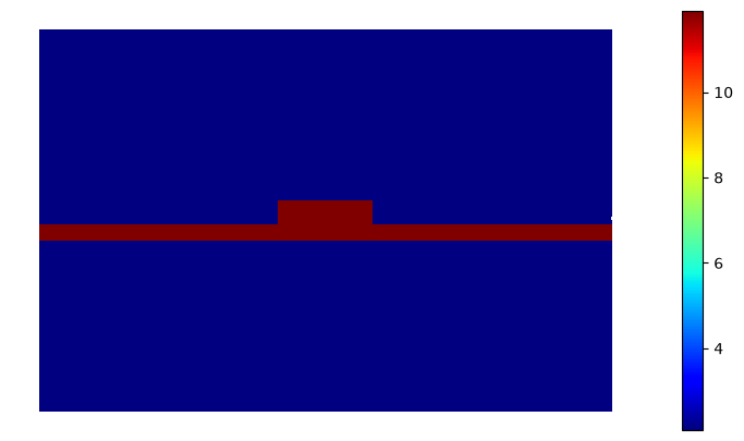
To define the epsilon, we proceed as for a regular waveguide, but we superimpose a voltage-dependent index of refraction based on the Soref Equations [2], [3]. These phenomenologically relate the change in complex index of refraction of silicon as a function of the concentration of free carriers. We model the spatial distribution of carriers according to the physics of a 1D PN junction in the depletion approximation. For more accurate results, full modeling of the silicon processing and physics through TCAD must be performed.
xpn = 0
NA = 1e18
ND = 1e18
V = 0
wavelength = 1.55


def define_index(mesh, V, xpn, NA, ND, wavelength):
    basis0 = Basis(mesh, ElementTriP0())
    epsilon = basis0.zeros(dtype=complex)
    for subdomain, n in {"core": 3.45, "slab": 3.45}.items():
        epsilon[basis0.get_dofs(elements=subdomain)] = n
    epsilon += basis0.project(
        lambda x: index_pn_junction(x[0], xpn, NA, ND, V, wavelength),
        dtype=complex,
    )
    for subdomain, n in {"clad": 1.444}.items():
        epsilon[basis0.get_dofs(elements=subdomain)] = n
    epsilon *= epsilon  # square now
    return basis0, epsilon


basis0, epsilon = define_index(mesh, V, xpn, NA, ND, wavelength)
basis0.plot(epsilon.real, colorbar=True).show()
basis0.plot(epsilon.imag, colorbar=True).show()
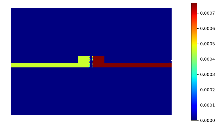
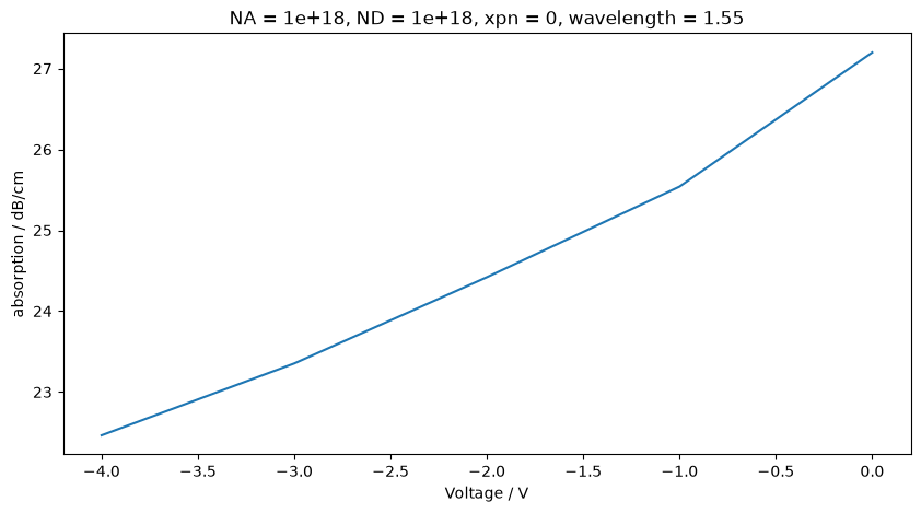
The index change is weak compared to the contrast between silicon and silicon dioxide, but it is accompanied by a change in absorption which is easier to observe. As voltage is increased, the region without charge widens, which is the mechanism behind depletion modulation:
V = -4
basis0, epsilon = define_index(mesh, V, xpn, NA, ND, wavelength)
basis0.plot(epsilon.imag, colorbar=True).show()

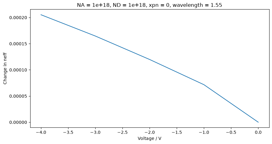
And now we can mode solve as before, and observe the change in effective index and absorption of the fundamental mode as a function of applied voltage for given junction position and doping levels:
voltages = [0, -1, -2, -3, -4]
neff_vs_V = []
for V in voltages:
    basis0, epsilon = define_index(mesh, V, xpn, NA, ND, wavelength)
    modes = compute_modes(basis0, epsilon, wavelength=wavelength, num_modes=1, order=2)
    neff_vs_V.append(modes[0].n_eff)
Bibliography#
Lukas Chrostowski and Michael Hochberg. Silicon Photonics Design: From Devices to Systems. Cambridge University Press, Cambridge, England, UK, March 2015. ISBN 978-1-10708545-9. URL: https://doi.org/10.1017/CBO9781316084168, doi:10.1017/CBO9781316084168.
R. Soref and B. Bennett. Electrooptical effects in silicon. IEEE J. Quantum Electron., 23(1):123–129, January 1987. URL: https://doi.org/10.1109/JQE.1987.1073206, doi:10.1109/JQE.1987.1073206.
Milos Nedeljkovic, Richard Soref, and Goran Z. Mashanovich. Free-Carrier Electrorefraction and Electroabsorption Modulation Predictions for Silicon Over the 1–14- µm Infrared Wavelength Range. IEEE Photonics J., 3(6):1171–1180, October 2011. URL: https://doi.org/10.1109/JPHOT.2011.2171930, doi:10.1109/JPHOT.2011.2171930.